Here are some pictures of the design:

A Google SketchUp Model of v0.1
I first made a quick mock up of the design to visualize how everything would fit and also to sell to the leaders of this museum project. I found that they were impressed with being able to see what design I had in my head and it was much more effective than me just describing it. As you can see in the design, I wanted to design a backpack device in which the LED matrix would sit on top of the circuit creating a nice handheld device. Also I will use polarized headers to make sure that users can only plug the wires in the correct way.

Schematic of version 0.1
This is where I made my big mistake in the circuit. I overlooked the fact that I was using an NPN darlington array to control the select side of my LED matrix and used them instead as if they were PNP which made the whole circuit pretty much worthless. Also you may notice that there was no ISP header to program the AVR chip and that was because I am currently using the Arduino platform and you can program just using the serial port and reset. However, this proved to be more difficult than it was worth so my next design will have an ISP header.

v0.1 PCB (Blue=bottom, Red=top)
Above is the PCB design for the board and I manually routed it to minimize the number of top traces. However I did route some top traces to the AVR chip which meant I couldn't use an IC socket which in the end was too bad because I ended up wasting an ATMEGA.


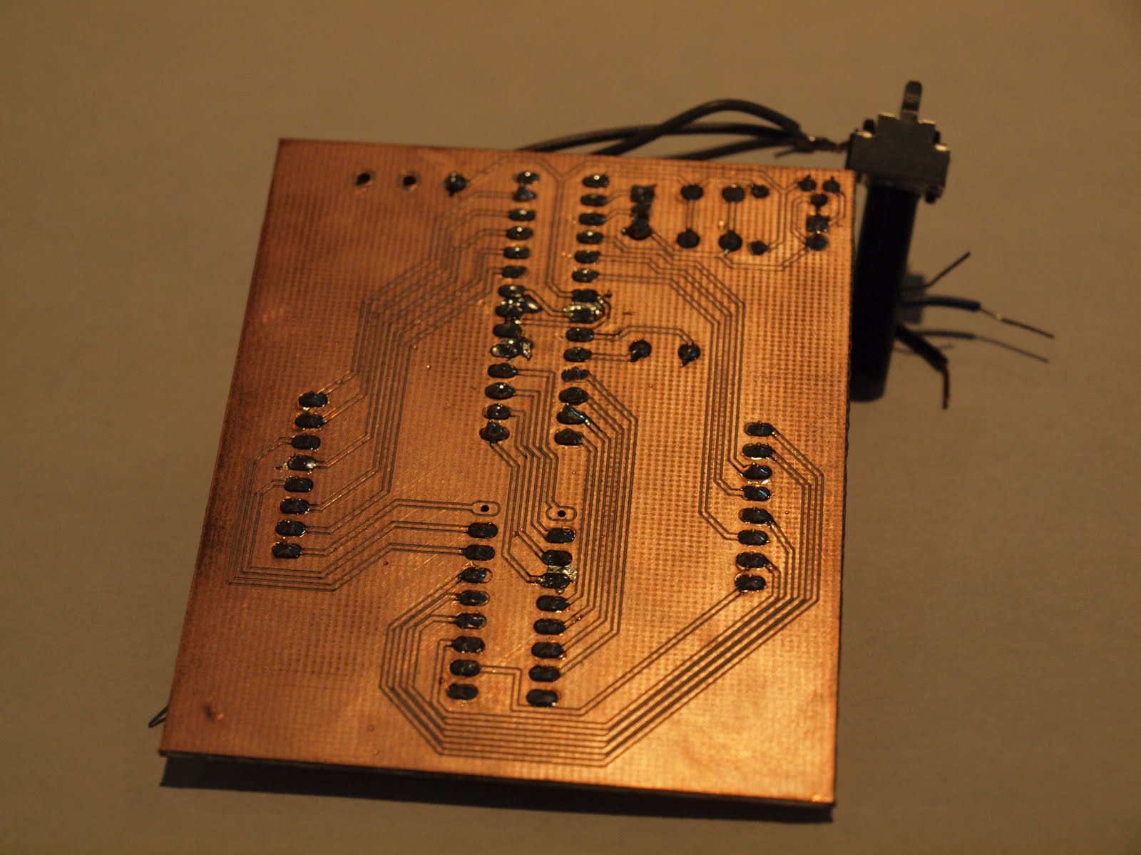

Here are some pictures of the finished prototype
I have learned several things from this prototype, one is always use an IC socket to minimize wasting expensive chips, include an ISP header especially when you are still developing the program, and always make sure you double check the datasheet of darlington arrays! I also learned a little bit more about soldering finding that all this time I had been using a solder wick incorrectly. I found that to use one effectively you place it over the solder joint you want to get rid of, heat it up, and then add a little solder to the top of the wick and then presto! the solder is gone.
Soon I will post my progress on the second prototype and hopefully I will have a video to demonstrate it.
No comments:
Post a Comment